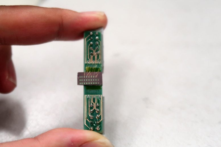
Close-up of the new MIT metasurface, or flat optical device patterned with some 100,000 nanoscale structures, that is integrated on a silicon chip and can be electrically activated. Credit: Photo Courtesy Yifei Zhang
Enormous potential range of applications.
Electrical Switch
In the Nature Nanotechnology paper, the MIT researchers describe using electrical currents to reversibly change the material structure—and therefore optical properties—of the new metasurface. In the past, they used bulky lasers or a furnace to supply the necessary heat. “This is important because we can now integrate the entire active optical device, along with the electrical switch, on a silicon chip to form a miniaturized optics platform,” says Juejun Hu, leader of the work and an Associate Professor of Materials Science and Engineering in DMSE.
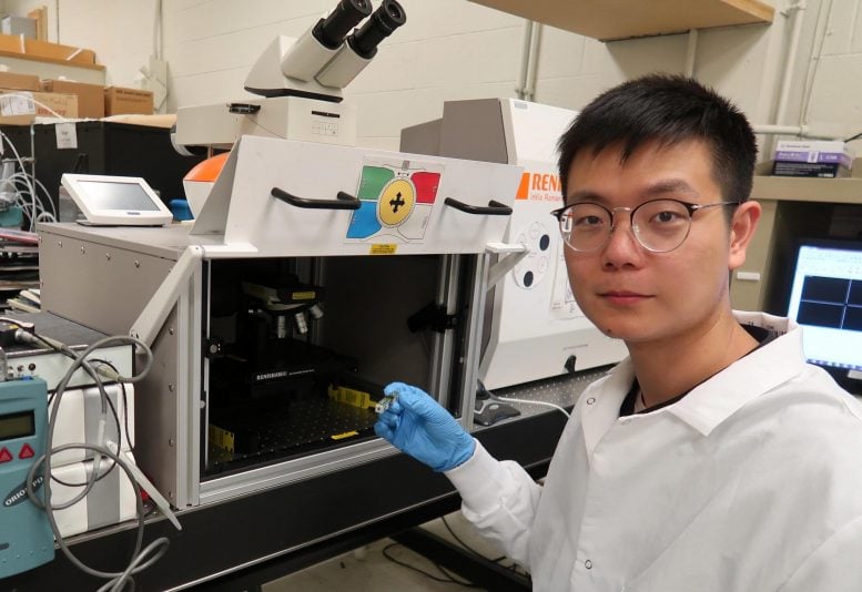
MIT Graduate Student Yifei Zhang holds the new metasurface, or flat optical device patterned with some 100,000 nanoscale structures, that is integrated on a silicon chip and can be electrically activated. Credit: Photo Courtesy Yifei Zhang
The team also reports demonstrating “a series of tunable optical functions using the platform,” Hu says. These include a beam steering device where “by switching the material to different [internal] structures, we can send light in one direction versus another, back and forth.” Beam steering is key to self-driving cars, although Hu emphasizes that the device he and colleagues demonstrated is still fairly rudimentary. “It’s more a proof of principle.”
In addition to Zhang and Hu, authors of the new paper are Junhao Liang, Bilal Azhar, Mikhail Y. Shalaginov, Skylar Deckoff-Jones, Carlos Rios, and Tian Gu, all of MIT DMSE; Clayton Fowler, Sensong An, and Hualiang Zhang of the University of Massachusetts, Lowell; Jeffrey B. Chou, Christopher M. Roberts, and Vladimir Liberman of MIT Lincoln Laboratory; Myungkoo Kang and Kathleen A. Richardson of the University of Central Florida, and Clara Rivero-Baleine of Lockheed Martin Corporation. Hu and Gu are also affiliated with MIT’s Materials Research Laboratory.
A New Material
Phase-change materials (PCMs) change their structure in response to heat. They are used commercially in rewritable CDs and DVDs. Explains Hu, “a laser beam changes the structure of the material locally, from amorphous to crystalline, and that change can be used to encode ones and zeros—digital information.”
However, conventional PCMs have limitations when it comes to optical applications. For one, they are opaque. They won’t let light pass through. “That motivated us to look into a new phase-change material for optical devices that is transparent,” Hu says. Earlier this year his team reported that adding another element, selenium, to a conventional PCM did the trick.
The new material, composed of germanium, selenium, antimony, and tellurium (GSST), is key to the new metasurface. The metasurface, in turn, is not just a thin film of GSST, it’s a film of GSST only about half a millimeter square patterned with some 100,000 nanoscale structures. And these, in turn, “allow you to control the propagation of light. So you can transform a collection of these nanostructures into, for example, a lens,” Hu says.
Harish Bhaskaran is a Professor at the