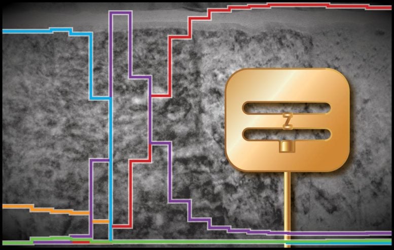
Scientists performed transmission electron microscopy and x-ray photoelectron spectroscopy (XPS) at Brookhaven Lab’s Center for Functional Nanomaterials and National Synchrotron Light Source II to characterize the properties of niobium thin films made into superconducting qubit devices at Princeton University. A transmission electron microscope image of one of these films is shown in the background; overlaid on this image are XPS spectra (colored lines representing the relative concentrations of niobium metal and various niobium oxides as a function of film depth) and an illustration of a qubit device. Through these and other microscopy and spectroscopy studies, the team identified atomic-scale structural and surface chemistry defects that may be causing loss of quantum information—a hurdle to enabling practical quantum computers. Credit: Brookhaven National Laboratory
Brookhaven Lab and Princeton scientists team up to identify sources of loss of quantum information at the atomic scale.
Engineers and materials scientists studying superconducting quantum information bits (qubits)—a leading

Anjali Premkumar
“Superconducting qubits are a promising quantum computing platform because we can engineer their properties and make them using the same tools used to make regular computers,” said Anjali Premkumar, a fourth-year graduate student in the Houck Lab at 
Andrew Houck
In this study, the team fabricated thin films of niobium metal through three different sputtering techniques. In sputtering, energetic particles are fired at a target containing the desired material; atoms are ejected from the target material and land on a nearby substrate. Members of the Houck Lab performed standard (direct current) sputtering, while Angstrom Engineering applied a new form of sputtering they specialize in (high-power impulse magnetron sputtering, or HiPIMS), where the target is struck with short bursts of high-voltage energy. Angstrom carried out two variations of HiPIMS: normal and with an optimized power and target-substrate geometry.
Back at Princeton, Premkumar made “transmon” qubit devices from the three sputtered films and placed them in a dilution refrigerator. Inside this refrigerator, temperatures can plunge to near 
Ignace Jarrige
Each device had different relaxation times. To understand these differences, the team performed microscopy and spectroscopy at the CFN and NSLS-II.
NSLS-II beamline scientists determined the oxidation states of niobium through x-ray photoemission spectroscopy with soft x-rays at the In situ and Operando Soft X-ray Spectroscopy (IOS) beamline and hard x-rays at the Spectroscopy Soft and Tender (SST-2) beamline. Through these spectroscopy studies, they identified various suboxides located between the metal and the surface oxide layer and containing a smaller amount of oxygen relative to niobium.
“We needed the high energy resolution at NSLS-II to distinguish the five different oxidation states of niobium and both hard and soft x-rays, which have different energy levels, to profile these states as a function of depth,” explained Jarrige. “Photoelectrons generated by soft x-rays only escape from the first few nanometers of the surface, while those generated by hard x-rays can escape from deeper in the films.”
At the NSLS-II Soft Inelastic X-ray Scattering (SIX) beamline, the team identified spots with missing oxygen atoms through resonant inelastic x-ray scattering (RIXS). Such oxygen vacancies are defects, which can absorb energy from qubits.
At the CFN, the team visualized film morphology using transmission electron microscopy and atomic force microscopy, and characterized the local chemical makeup near the film surface through electron energy-loss spectroscopy.
Sooyeon Hwang
“The microscope images showed grains—pieces of individual crystals with atoms arranged in the same orientation—sized larger or smaller depending on the sputtering technique,” explained coauthor Sooyeon Hwang, a staff scientist in the CFN Electron Microscopy Group. “The smaller the grains, the more grain boundaries, or interfaces where different crystal orientations meet. According to the electron energy-loss spectra, one film had not just oxides on the surface but also in the film itself, with oxygen diffused into the grain boundaries.”
Their experimental findings at the CFN and NSLS-II revealed correlations between qubit relaxation times and the number and width of grain boundaries and concentration of suboxides near the surface.
“Grain boundaries are defects that can dissipate energy, so having too many of them can affect electron transport and thus the ability of qubits to perform computations,” said Premkumar. “Oxide quality is another potentially important parameter. Suboxides are bad because electrons are not happily paired together.”
Going forward, the team will continue their partnership to understand qubit coherence through C2QA. One research direction is to explore whether relaxation times can be improved by optimizing fabrication processes to generate films with larger grain sizes (i.e., minimal grain boundaries) and a single oxidation state. They will also explore other superconductors, including tantalum, whose surface oxides are known to be more chemically uniform.
“From this study, we now have a blueprint for how scientists who make qubits and scientists who characterize them can collaborate to understand the microscopic mechanisms limiting qubit performance,” said Premkumar. “We hope other groups will leverage our collaborative approach to drive the field of superconducting qubits forward.”
Reference: “Microscopic relaxation channels in materials for superconducting qubits” by Anjali Premkumar, Conan Weiland, Sooyeon Hwang, Berthold Jäck, Alexander P. M. Place, Iradwikanari Waluyo, Adrian Hunt, Valentina Bisogni, Jonathan Pelliciari, Andi Barbour, Mike S. Miller, Paola Russo, Fernando Camino, Kim Kisslinger, Xiao Tong, Mark S. Hybertsen, Andrew A. Houck and Ignace Jarrige, 1 July 2021, Communications Materials.DOI: 10.1038/s43246-021-00174-7
This work was supported by the DOE Office of Science, National Science Foundation Graduate Research Fellowship, Humboldt Foundation, National Defense Science and Engineering Graduate Fellowship, Materials Research Science and Engineering Center, and Army Research Office. This research used resources of the Electron Microscopy, Proximal Probes, and Theory and Computation Facilities at the CFN, a DOE Nanoscale Science Research Center. The SST-2 beamline at NSLS-II is operated by the National Institute of Standards and Technology.