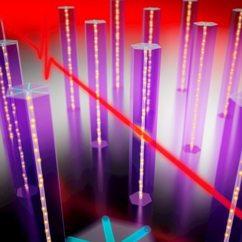
Terahertz spectroscopy measurements showed that the strained core of semiconductor nanowires can host fast moving electrons, a concept that could be employed for a new generation of nano-transistors. Credit: HZDR/Juniks
Nanowires under tension create the basis for ultrafast transistors.
Smaller chips, faster computers, less energy consumption. Novel concepts based on semiconductor nanowires are expected to make transistors in microelectronic circuits better and more efficient. Electron mobility plays a key role in this: The faster electrons can accelerate in these tiny wires, the faster a transistor can switch and the less energy it requires. A team of researchers from the
What started out as a theoretical prediction has now been proven experimentally by the researchers in the recently published study. “We knew that the electrons in the core ought to be even more mobile in the tensile-strained crystal structure. But what we did not know was the extent to which the wire shell would affect electron mobility in the core. The core is extremely thin, allowing electrons to interact with the shell and be scattered by it,” remarked Dimakis. A series of measurements and tests demonstrated this effect: Despite interaction with the shell, electrons in the core of the wires under investigation moved approximately thirty percent faster at room temperature than electrons in comparable nanowires that were strain-free or in bulk gallium arsenide.
Revealing the core
The researchers measured electron mobility by applying contactless optical spectroscopy: Using an optical laser pulse, they set electrons free inside the material. The scientists selected the light-pulse energy such that the shell seems practically transparent to the light, and free electrons are only produced in the wire core. Subsequent high-frequency terahertz pulses caused the free electrons to oscillate. “We practically give the electrons a kick and they start oscillating in the wire,” explained PD Dr. Alexej Pashkin, who optimized the measurements for testing the core-shell nanowires under investigation in collaboration with his team at the HZDR.
Comparing the results with models reveals how the electrons move: The higher their speed and the fewer obstacles they encounter, the longer the oscillation lasts. “This is actually a standard technique. But this time we did not measure the whole wire – comprising the core and the shell – but only the tiny core. This was a new challenge for us. The core accounts for around one percent of the material. In other words, we excite about a hundred times fewer electrons and get a signal that is a hundred times weaker,” stated Pashkin.
Consequently, the choice of sample was also a critical step. A typical sample contains an average of around 20,000 to 100,000 nanowires on a piece of substrate measuring roughly one square millimeter. If the wires are spaced even closer together on the sample, an undesirable effect can occur: Neighboring wires interact with each other, creating a signal similar to that of a single, thicker wire, and distorting the measurements. If this effect is not detected, the electron velocity obtained is too low. To rule out such interference, the Dresden research team carried out additional modelling as well as a series of measurements for nanowires with different densities.
Prototypes for fast transistors
Trends in microelectronics and the semiconductor industry increasingly demand smaller transistors that switch ever faster. Experts anticipate that novel nanowire concepts for transistors will also make inroads into industrial production over the next few years. The development achieved in Dresden is particularly promising for ultra-fast transistors. The researchers’ next step will be to develop the first prototypes based on the studied nanowires and to test their suitability for use. To do this, they intend to apply, test and enhance metallic contacts on the nanowires, as well as testing the doping of nanowires with silicon and optimizing manufacturing processes.
Reference: “High electron mobility in strained GaAs nanowires” by Leila Balaghi, Si Shan, Ivan Fotev, Finn Moebus, Rakesh Rana, Tommaso Venanzi, René Hübner, Thomas Mikolajick, Harald Schneider, Manfred Helm, Alexej Pashkin and Emmanouil Dimakis, 17 November 2021, Nature Communications.DOI: 10.1038/s41467-021-27006-z