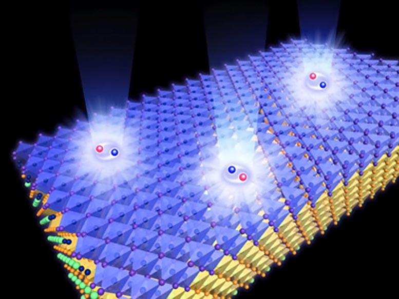
Figure 1: A thin film of cuprous iodide crystals (blue) on an indium arsenide substrate (yellow). The sample’s purity was tested by shining photons onto the surface to create electron–hole pairs (red and blue spheres) and monitoring the light that was emitted (white rays). Credit: © 2021 RIKEN Center for Emergent Matter Science
Better optoelectronic devices could be realized using a high-quality film of cuprous iodide.
A defect-free thin film of cuprous iodide—made up of just one crystal—has been fabricated by RIKEN physicists1. The atomically flat sample is a boost for producing better semiconductors.
Semiconductors lie at the heart of many optoelectronic devices including lasers and light-emitting diodes (LEDs). Engineers would love to use cuprous iodide—an example of a halide compound—for semiconductors because it is an excellent conductor that is stable above room temperature. The trouble is that it is tough to fabricate a genuinely thin film of cuprous iodide without impurities. The usual method involves depositing the film from a solution. “But a solution process can’t make a high-quality thin film from cuprous iodide,” says Masao Nakamura of the RIKEN Center for Emergent Matter Science.
Instead, Nakamura and his co-workers used an alternative technique known as molecular beam epitaxy, in which the film is gradually grown on top of a substrate, at an elevated temperature, and in a vacuum. Molecular beam epitaxy is already commonly employed in manufacturing semiconductors. But it is hard to use for cuprous iodide because the material is highly volatile—meaning that it easily evaporates during the process, rather than settling into a film. To overcome this difficulty, the team began growing their film at a lower temperature and then increased the temperature. “This two-step process we newly developed was highly effective,” says Nakamura.
The team had another trick to raise the quality of their film. They chose indium arsenide as the substrate since its lattice spacing is very similar to that of cuprous iodide. “If the lattice spacing is not well matched, many defects will form in the material,” explains Nakamura.
Nakamura and his colleagues then tested the purity of their sample using a technique called photoluminescence spectroscopy, which involves firing photons, or particles of light, at the surface of the material. These photons are absorbed by the material, exciting its electrons to a higher energy state and causing them to emit new photons (Fig. 1). Monitoring the emitted light allowed the team to determine that they had created a single-crystal film, free from defects. “We expected the quality to improve using our method,” says Nakamura. “But the results exceeded our expectations.”
Nakamura and his team now plan to sandwich together semiconductors made of different halides and investigate new properties that arise. “We will explore emerging novel functionalities and physics at the halide interfaces,” says Nakamura.
Reference: “Heteroepitaxial growth of wide bandgap cuprous iodide films exhibiting clear free-exciton emission” by S. Inagaki, M. Nakamura, Y. Okamura, M. Ogino, Y. Takahashi, L. C. Peng, X. Z. Yu, Y. Tokura and M. Kawasaki, 5 January 2021, Applied Physics Letters.DOI: 10.1063/5.0036862