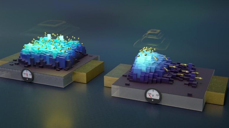
The device uses a simple electric diode to manipulate qubits inside a commercial silicon wafer. Credit: Second Bay Studios/Harvard SEAS
By utilizing traditional semiconductor devices, researchers have unlocked new potentials in quantum communication, pushing us closer to realizing the vast potential of the quantum internet.
Building the quantum internet could be significantly simplified by leveraging existing telecommunications technologies and infrastructure. In recent years, researchers have identified defects in silicon—a widely used semiconductor material—that hold the potential for transmitting and storing quantum information across the prevalent telecommunications wavelengths. These silicon defects might just be the prime contenders to host qubits for efficient quantum communications.
Exploring Quantum Defects in Silicon
“It’s still a Wild West out there,” said Evelyn Hu, the Tarr-Coyne Professor of Applied Physics and of Electrical Engineering at the Harvard John A. Paulson School of Engineering and Applied Sciences (SEAS). “Even though new candidate defects are a promising quantum memory platform, there is often almost nothing known about why certain recipes are used to create them, and how you can rapidly characterize them and their interactions, even in ensembles. And ultimately, how can we fine-tune their behavior so they exhibit identical characteristics? If we are ever to make a technology out of this wide world of possibilities, we must have ways to characterize them better, faster, and more efficiently.”
Now, Hu and a team of researchers have developed a platform to probe, interact with and control these potentially powerful quantum systems. The device uses a simple electric diode, one of the most common components in semiconductor chips, to manipulate qubits inside a commercial silicon wafer. Using this device, the researchers were able to explore how the defect responds to changes in the electric field, tune its wavelength within the telecommunications band and even turn it on and off.
“If we are ever to make a technology out of this wide world of possibilities, we must have ways to characterize them better, faster and more efficiently.”
— Evelyn Hu, Tarr-Coyne Professor of Applied Physics and of Electrical Engineering
Harnessing Defects for Quantum Communications
“One of the most exciting things about having these defects in silicon is that you can use well-understood devices like diodes in this familiar material to understand a whole new quantum system and do something new with it,” said Aaron Day, a Ph.D. candidate at SEAS. Day co-led the work with Madison Sutula, a research fellow at Harvard.
While the research team used this approach to characterize defects in silicon, it could be used as a diagnostic and control tool for defects in other material systems.
The research is published in SciTechDaily