Researchers have developed an innovative phase change memory device that promises low power consumption and reduced manufacturing costs. This development, potentially replacing DRAM and NAND flash memory, is notable for its efficiency and could significantly impact the future of memory and neuromorphic computing technology. Credit: SciTechDaily.com
Phase Change Memory
A memory device that stores and/or processes information by changing the crystalline states of materials to be amorphous or crystalline using heat, thereby changing its resistance state.
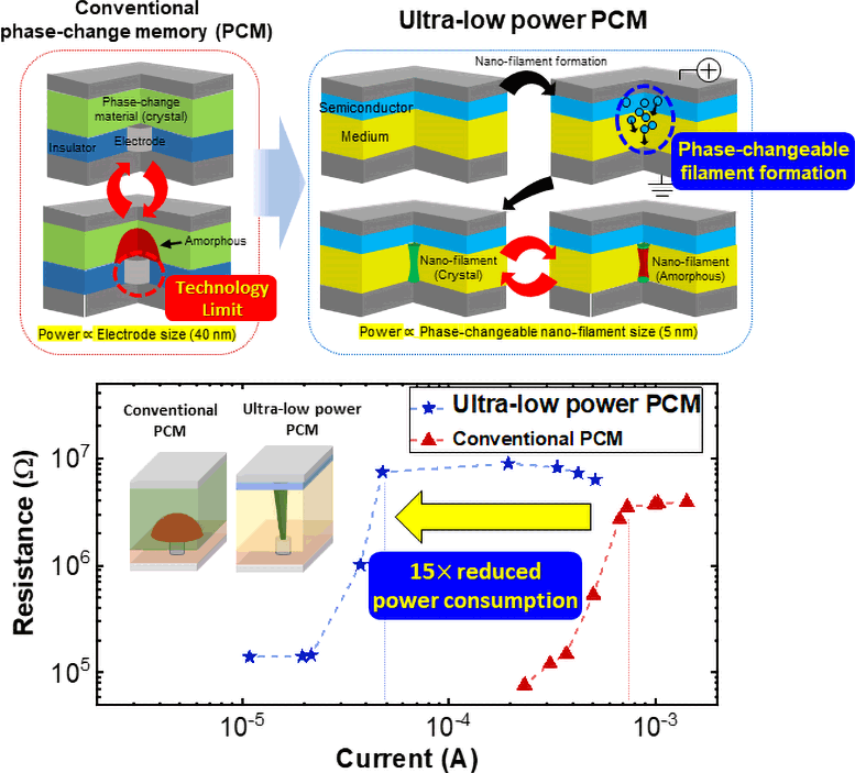
Existing phase change memory has problems such as an expensive fabrication process for making highly scaled devices and requiring a substantial amount of power for operation. To solve these problems, Professor Choi’s research team developed an ultra-low power phase change memory device by electrically forming a very small nanometer (nm) scale phase changeable filament without expensive fabrication processes. This new development has the groundbreaking advantage of not only having a very low processing cost but also enabling operating with ultra-low power consumption.
DRAM, one of the most popularly used memory, is very fast, but has volatile characteristics in which data disappears when the power is turned off. NAND flash memory, a storage device, has relatively slow read/write speeds, but it has non-volatile characteristic that enables it to preserve the data even when the power is cut off.

Figure 1. Illustrations of the ultra-low power phase change memory device developed through this study and the comparison of power consumption by the newly developed phase change memory device compared to conventional phase change memory devices. Credit: KAIST Emerging Nano Technology and Integrated Systems
Phase change memory, on the other hand, combines the advantages of both DRAM and NAND flash memory, offering high speed and non-volatile characteristics. For this reason, phase change memory is being highlighted as the next-generation memory that can replace existing memory, and is being actively researched as a memory technology or neuromorphic computing technology that mimics the human brain.
However, conventional phase change memory devices require a substantial amount of power to operate, making it difficult to make practical large-capacity memory products or realize a neuromorphic computing system. In order to maximize the thermal efficiency for memory device operation, previous research efforts focused on reducing the power consumption by shrinking the physical size of the device through the use of the state-of-the-art lithography technologies, but they were met with limitations in terms of practicality as the degree of improvement in power consumption was minimal whereas the cost and the difficulty of fabrication increased with each improvement.
In order to solve the power consumption problem of phase change memory, Professor Shinhyun Choi’s research team created a method to electrically form phase change materials in extremely small area, successfully implementing an ultra-low-power phase change memory device that consumes 15 times less power than a conventional phase change memory device fabricated with the expensive lithography tool.
Professor Shinhyun Choi expressed strong confidence in how this research will span out in the future in the new field of research saying, “The phase change memory device we have developed is significant as it offers a novel approach to solve the lingering problems in producing a memory device at a greatly improved manufacturing cost and energy efficiency. We expect the results of our study to become the foundation of future electronic engineering, enabling various applications including high-density three-dimensional vertical memory and neuromorphic computing systems as it opened up the possibilities to choose from a variety of materials.” He went on to add, “I would like to thank the National Research Foundation of Korea and the National NanoFab Center for supporting this research.”
This study, in which See-On Park, a student of MS-PhD Integrated Program, and Seokman Hong, a doctoral student of the School of Electrical Engineering at KAIST, participated as first authors, was published on April 4 in the April issue of the renowned international academic journal Nature.
Reference: “Phase-change memory via a phase-changeable self-confined nano-filament” by See-On Park, Seokman Hong, Su-Jin Sung, Dawon Kim, Seokho Seo, Hakcheon Jeong, Taehoon Park, Won Joon Cho, Jeehwan Kim and Shinhyun Choi, 3 April 2024, Nature.DOI: 10.1038/s41586-024-07230-5
This research was conducted with support from the Next-Generation Intelligent Semiconductor Technology Development Project, PIM AI Semiconductor Core Technology Development (Device) Project, Excellent Emerging Research Program of the National Research Foundation of Korea, and the Semiconductor Process-based Nanomedical Devices Development Project of the National NanoFab Center.