Intel is hard at work executing on its IDM 2.0 strategy, with a stated goal to deliver five process node advancements in four years. The company recently brought us and other members of the tech press out to its facilities in Malaysia to see its progress first-hand. Intel has several factories in Penang and Kulim which handle a variety of assembly and test processes, including die sort and die prep, packaging, as well as the manufacturing of Intel’s internal test equipment.

Arriving At Intel Malaysia
Malaysia is the home of Intel’s first offshore facility, built in 1972. The first assembly plant, A1, was staffed by 100 employees on a 5-acre parcel. Intel’s investment in Malaysia now spans 15,000 employees across 900,000 square feet of manufacturing space split between Penang and Kulim. The manufacturing space is continuing to grow, and Intel says it will soon surpass two million square feet once its ongoing expansions are completed.
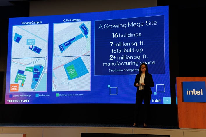
Intel still controls the original A1 plant site, but it has been torn down to make way for the new Pelican advanced packaging facility.
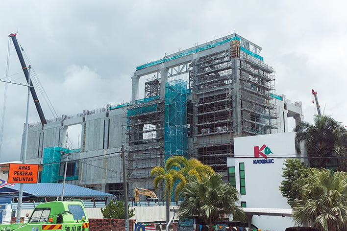
That project is well underway, and we were able to see the construction in progress as we made our way to PG8 as part of our tour. It is currently on-track to be production-ready in 2025.
Touring Intel’s Malaysia Facilities
Our tour started at PG16’s Design and Development Lab where the company conducts validation testing on early silicon samples, but perhaps it makes more sense to begin with how silicon arrives in Malaysia in the first place. The process starts across the Penang Bridge in Kulim at KMDSDP (Die Sort, Die Prep).
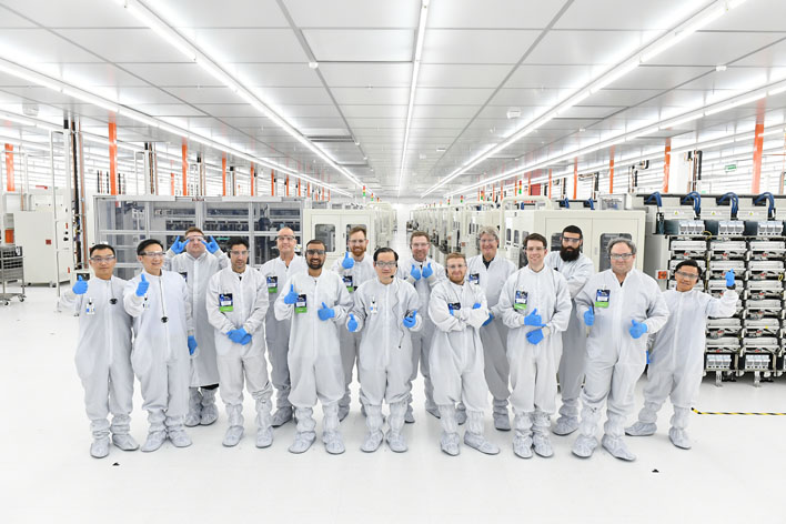
Before we could enter any of these cleanroom facilities, we had to don varying levels of protective cleanroom coverings. This typically consisted of a cleanroom smock and sometimes hair and beard nets, but could include the full “bunny suit” with leg and shoe coverings as well.
Slicing Wafers To Make Dies
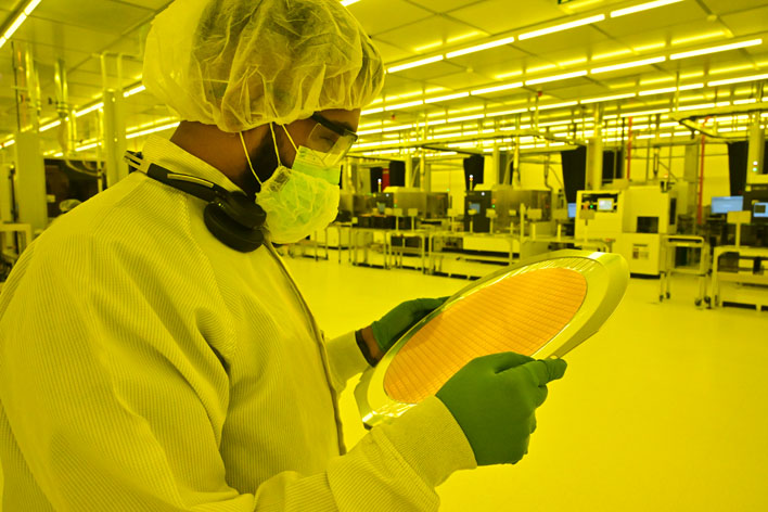
Completed wafers arrive at KMDSDP where the individual chips need to be processed prior to assembly. Wafers are first affixed to a clear mylar tape backing. UV light causes the mylar backing to lose its stickiness, so this takes place in a portion of the factory that is bathed in amber light. The mylar is slightly stretchy, but mostly ensures that the dies will remain in-position as they are separated.
Some chips, such as those destined for mobile devices, need to be thinned at this point. These wafers are first mounted face-down and then the back side is ground down to the target thickness. The wafer is then inverted onto another mylar backing to proceed as normal.
Die separation is a multi-step process. The chip divisions are pre-scored with lasers, though we were unable to see this process in action as it takes place behind protective curtains. This is followed by another machine which literally saws the wafers apart, a process called singulation. The machine is equipped with two diamond-tipped blades to improve throughput. The blades cut cleanly through the wafer and partially into the mylar backing as chilled water flows over the process to both help remove debris and to prevent thermal expansion from damaging the delicate chips. The system monitors factors like blade integrity to ensure cuts remain clean and precise.
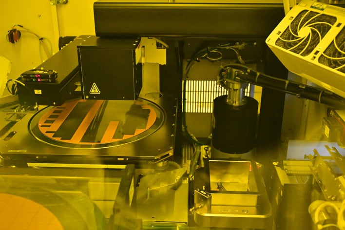
From here, another machine loads the singulated wafers, then systematically extracts each die onto a tray, called pick & place. It uses a brief UV flash to weaken the mylar bond, then it applies a vacuum to the mylar side, and via a robotic arm, to the top of the die. The mylar-side vacuum prevents it from sticking as a series of pins push through to free the chip. The robotic arm then guides each die to a designated position on the tray.
Intel notes that these trays are effectively universal across their products. There are no sockets for chips to slot into. Instead, the bed of the tray has a white material perforated with a hexagonal grid of holes. It seems these provide a light suction pressure as the chips are placed which allows the trays to be moved around the facilities without dies getting jostled. More importantly, the generalized design helps Intel’s production remain flexible particularly as it shifts into a disaggregated approach to manufacturing.
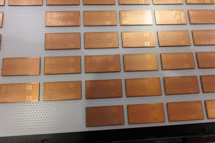
At this point, Intel has a loaded tray of fresh dies, but needs to characterize them before processing can continue. The trays are loaded into a lot, which is a sort of plastic housing for trays being shuttled around the facility.
Testing And Characterizing Freshly Separated Dies
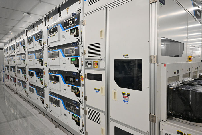
Intel tests the dies individually using a bus-sized machine. One side is populated by twenty test cells, each weighing about 1,000 pounds. These each measure about five feet wide and five feet deep, and a couple feet tall. Lots are loaded at one end, then a robotic system in the center distributes trays of chips to available test cells, something akin to an enormous vending machine. Each test cell will take in a tray, then automatically work through the chips loaded on it to test and characterize each one.
The test cells operate independently, so any given unit can test different products or even be taken offline individually for maintenance. Intel has a nearly floor-to-ceiling lifting jig it uses to move these cells around the facility as needed. The jig is an impressive marvel of engineering in its own right, as it floats just above the floor on a cushion of air. Intel has covered most of the ground with a sheet of plastic to create a better seal. This prevents the weight of the test cell and jig combined from damaging the floor, and also makes it surprisingly maneuverable. It can be guided around with a single hand, though care is certainly taken to prevent it from careening into the rows of test equipment around.
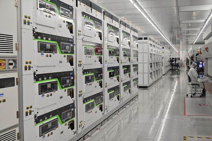
The test processes are run effectively autonomously. Stations are setup where a worker can monitor several rows of testers at once. We watched as one of the workers effortlessly cycled between four monitors of windows and menus with the speed and precision of a seasoned Starcraft professional.
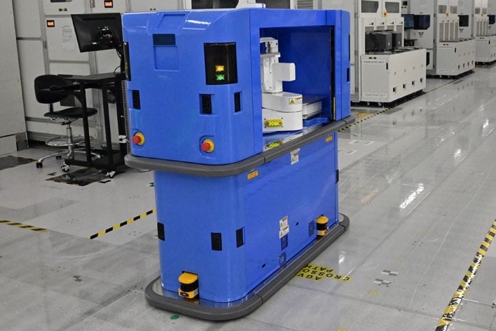
Apart from monitoring and maintenance, little human interaction is needed. Lots are shuffled between the test equipment and the storage spaces around the perimeter by automated guidance vehicles (AGVs). The system constantly evaluates which test cells are available and where to select the lots with the highest throughput potential, rather than simply testing on a first in, first out basis. These AGVs navigate independently along paths without set routes and play a chorus of tones (like an ice cream truck) continuously to ensure their presence is known by any nearby humans.
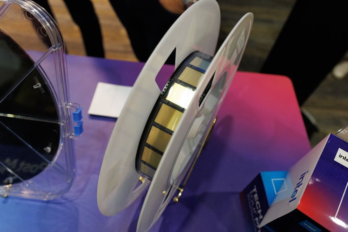
Tested trays return to a reeling machine next to the Pick & Place machine. At this point, chips have been characterized and binned to a particular SKU. As trays are sorted, a robotic arm moves individual chips onto different reels according to its associated SKU. The reels sandwich the chips between two layers of tape for safe transport with sprocket hole perforations along the sides that makes them look like film reels at first glance. Dies that have not passed testing are moved aside at this stage and collected for disposal or recycling.
Source: hothardware.com