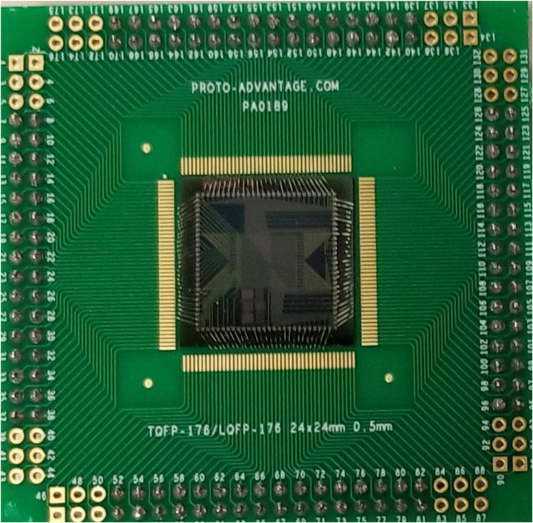
A memory chip was made of transistors with carbon nanotubes that maintained their electrical properties and memory after being bombarded by high amounts of radiation. Credit: Adapted from ACS Nano 2021, DOI: 10.1021/acsnano.1c04194
Space missions, such as
To do this, the researchers deposited carbon nanotubes on a silicon wafer as the semiconducting layer in field-effect transistors. Then, they tested different transistor configurations with various levels of shielding, consisting of thin layers of hafnium oxide and titanium and platinum metal, around the semiconducting layer.
The team found that placing shields both above and below the carbon nanotubes protected the transistor’s electrical properties against incoming radiation up to 10 Mrad — a level much higher than most silicon-based radiation-tolerant electronics can handle. When a shield was only placed beneath the carbon nanotubes, they were protected up to 2 Mrad, which is comparable to commercial silicon-based radiation-tolerant electronics.
Finally, to achieve a balance between fabrication simplicity and radiation robustness, the team built static random-access memory (SRAM) chips with the bottom shield version of the field-effect transistors. Just as with experiments performed on the transistors, these memory chips had a similar X-ray radiation threshold as silicon-based SRAM devices.
These results indicate that carbon nanotube field-effect transistors, especially double-shielded ones, could be a promising addition to next-generation electronics for space exploration, the researchers say.
Reference: “Carbon Nanotubes for Radiation-Tolerant Electronics” by Pritpal S. Kanhaiya, Andrew Yu, Richard Netzer, William Kemp, Derek Doyle and Max M. Shulaker, 27 October 2021, ACS Nano.DOI: 10.1021/acsnano.1c04194
The authors acknowledge funding from the U.S. Air Force Research Laboratory and Analog Devices, Inc.