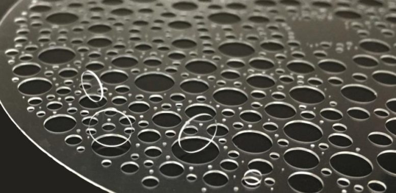
Fused silica wafer with thickness of 350 um with high-quality glass vias of diameters between 0.25 mm and 6 mm fabricated by selective laser etching. From 10.1117/1.OE.60.2.025105. Credit: Daniel Flamm et al.
Industrial-grade materials processing on the sub-micron scale is enabled by spatially structured ultrashort laser pulses.
If light is strongly concentrated in time and space, resulting in extreme photon densities, it can enable interaction with all conceivable materials. By using these ultrashort laser foci, even transparent materials can be modified, even though they ordinarily would not interact. Short, focused laser pulses can overcome this transparency and allow energy to be deposited completely contact-free. The exact response of the material to the radiation can be very diverse, ranging from marginal refractive index changes to destructive microscale explosions that evacuate entire areas.
Using the laser pulses for optical machining allows for equally diverse material modification, such as separating or joining using the same laser system. Due to the extremely short exposure time and low degree of thermal diffusion, neighboring areas remain completely unaffected, enabling true micron-scale material processing.
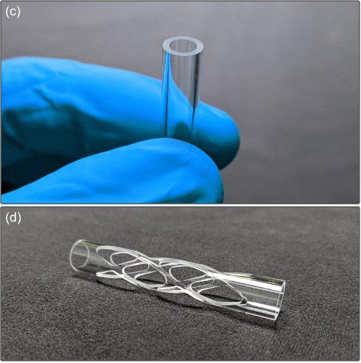
In “Structured light for ultrafast laser micro- and nanoprocessing” by Daniel Flamm et al., various concepts are presented for manipulating the spatial distribution of laser light at the focus in such a way that particularly efficient and, thus, industrially suitable processing strategies can be applied. For example, customized nondiffracting beams, generated by holographic axicons, can be used to modify glass sheets up to millimeter scales using single-passes and feed rates of up to a meter per second. The application of this concept to curved substrates and the development of a laser-based glass tube cutting is a groundbreaking advance. This capability has long been needed by the medical industry for the fabrication of glass items such as syringes, vials and ampoules. The machined surfaces produce excellent edge quality and are free from micro debris, to meet the demands of the consumer and medical industry.

Cutting of glass tubes with complex inner and outer contours. Credit: Daniel Flamm et al.
This paper also demonstrates the potential of a newly introduced 3D-beam-splitter concept. Here, 13 identical copies of the original focus are distributed across the three-dimensional working volume using a single focusing objective, serving to increase the effective volume of a weld seam. The material’s response to the pulse is directly measured using transverse pump-probe microscopy confirming a successful energy deposition with 13 individual absorption zones. The conducted experiment represents a prime example of three-dimensional parallel processing based on structured light concepts and demonstrates increased throughput scaling by exploiting the performance of high-power, ultrashort pulsed laser systems.
The broad accessibility of liquid crystal displays and their application to beam shaping using holography has also led the materials processing community to adopt structured light concepts. However, these approaches have not yet been translated into industrial processing, mainly because such displays cannot handle high optical powers and energies as well as the high programming effort required to construct digital holograms.

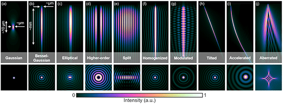
Menu of diffracting, nondiffracting, and quasi nondiffracting beams designed for transparent materials processing. Credit: Daniel Flamm, et al.
This paper was able to report significant progress on this front. With the presented double illumination concept, the liquid crystal display modulates both amplitude and phase of the illuminating optical field. By applying digital amplitude masks, arbitrary intensity profiles can be generated, offering benefits for formation of high spatial frequency, fine metal masks. The adapted flat-top intensity profiles depicted in the manuscript are generated without using complex Fourier coding strategies, making the concept a promising candidate for future digital optical processing heads.
Reference: “Structured light for ultrafast laser micro- and nanoprocessing” by Daniel Flamm, Daniel G. Grossmann, Marc Sailer, Myriam Kaiser, Felix Zimmermann, Keyou Chen, Michael Jenne, Jonas Kleiner, Julian Hellstern, Christoph Tillkorn, Dirk H. Sutter and Malte Kumkar, 24 February 2021, Optical Engineering.DOI: 10.1117/1.OE.60.2.025105