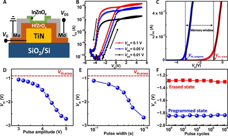
Ferroelectric memory is a well-researched topic in the past decade due to its capacity for higher speed, lower power consumption and longer endurance, compared to conventional flash memory. The performance of ferroelectric memory can be compromised substantially due to the formation of unwanted interfacial layers during the development of ferroelectric memory-based on perovskite oxides-on-silicon. In a new report, Min-Kyu Kim, and a team of scientists in materials science and engineering at the Pohang University of Science and Technology in Korea, demonstrated a unique strategy by applying hafnia-based ferroelectrics and oxide semiconductors for three-dimensional (3-D) integration. The strategy achieved memory performance beyond the conventional flash memory and exceeded those achieved by perovskite ferroelectric memories. The team then simulated the devices to confirm the ability to realize ultra-high-density 3-D memory integration.
Flash memory
Flash memory devices are presently in use for massive data storage across mobile devices and servers through floating-gates or charge-trap memory transistors based on electron-tunneling through a tunnel oxide. The electron-tunneling process requires voltage pulses with high amplitude and long duration; however, existing flash memory devices only possess a high functional voltage approximating 20 volts and a slow speed coupled with limited endurance. The process further required high deposition and annealing temperatures to form channel and oxide layers. Scientists therefore developed a range of emerging memory devices to overcome these limits, however, there are no existing alternatives to current flash memory in order to obtain fast functionality at a low power. In the meantime, researchers have developed hafnia-based ferroelectric materials due to their complementary metal-oxide semiconductor (CMOS) compatibility, low power consumption and fast switching speed.
Kim et al. presented unique methods to overcome key issues of ferroelectric memory transistors by introducing indium zinc oxide (InZnOx) as the semiconductor layer and zirconium-doped hafnium oxide (HfZrOx) as the ferroelectric layer to obtain high-performance memories. The outcomes resulted in an operational speed several hundred times faster, and an operational voltage four times lower compared to existing flash memory. All processes could be conducted below 400 degrees Celsius with integrated ferroelectric memory devices that are CMOS compatible to achieve commercialization milestones including NAND (NOT-AND gate) flash arrays and 3-D vertical structures. The nanoscale 3-D vertical flash memory showed excellent performances for ultra-high-density 3-D flash memory in the future.
Developing a high-performance ferroelectric transistor
Kim et al. first confirmed the ferroelectric properties of zirconium-doped hafnium oxide by developing a capacitor with a titanium nitride/zirconium-doped hafnium oxide/ titanium nitride (TiN/HfZrOx/TiN) structure, and measured the polarization-electric field characteristics of the 24-nm thick material. The coercive electric field of the material was larger than that of ferroelectric perovskite oxides and advantageous in ferroelectric transistors since the large coercive electric fields comparatively led to a larger memory window. The team next confirmed the ferroelectricity of zirconium-doped hafnium oxide using piezoresponse force microscopy and capacitance-voltage measurements to confirm their ferroelectric nature for endurance characteristics. The scientists tested the feasibility of the integration strategies using ferroelectric thin-film transistors (FeTFTs) with a bottom-contact structure developed using atomic layer deposition-based zirconium-doped hafnium oxide and indium zinc oxide (HfZrOx and InZnOx). To confirm the reliability of these ferroelectric thin-film transistors, Kim et al. also tested their endurance properties. The robust endurance character of the setup originated from its metal-ferroelectric semiconductor structure without an interfacial layer. Compared to previous memory devices such as charge-trap memory and perovskite oxide-based ferroelectric transistors, the use of HfZrOx and InZnOx resulted in lower functional voltage, faster operation speed and lower processing temperature.
Memory operation of integrated ferroelectric NAND
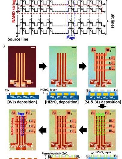
Flash memory cells are generally connected in a hierarchy to allow efficient access. Typically, a number of cells are connected in a string, organized in blocks, where each string in the block is connected to a separate bitline (BL) and the control gate of each cell in the string can be connected to a wordline (WL). Structurally, ferroelectric NAND (FeNAND) flash memory arrays are similar to NAND flash devices, while differing only by the type of memory cells. For example, FeNAND flash memory arrays typically use ferroelectric transistors, while NAND flashes used conventional flash memory. All FeNAND strings shared a source line (SL), while each NAND string was connected to bitlines. The team developed a 4 by 4 FeNAND array by including ferroelectric thin-film transistors with a ferroelectric zirconium-doped hafnium oxide layer and indium zinc oxide channel layer in a CMOS compatible fabrication process.
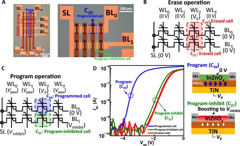
The completed NAND array contained 16 memory cells to demonstrate its program operation. Program disturbances could occur in the setup if unwanted programming occurred in memory cells during operation. To avoid this phenomenon, Kim et al. used a program-inhibit operation method by applying a program-inhibit pulse. During the experiments, all 16 memory cells in the FeNAND array functioned without fail and the results confirmed NAND memory operation to be successful with an array of ferroelectric thin-film transistors (FeTFTs). The team also developed FeNAND arrays on a silicon wafer and measured the program and erase operation of nine memory cells, where the experimental results and those simulated with the technology computer-aided design (TCAD) tool agreed with each other.
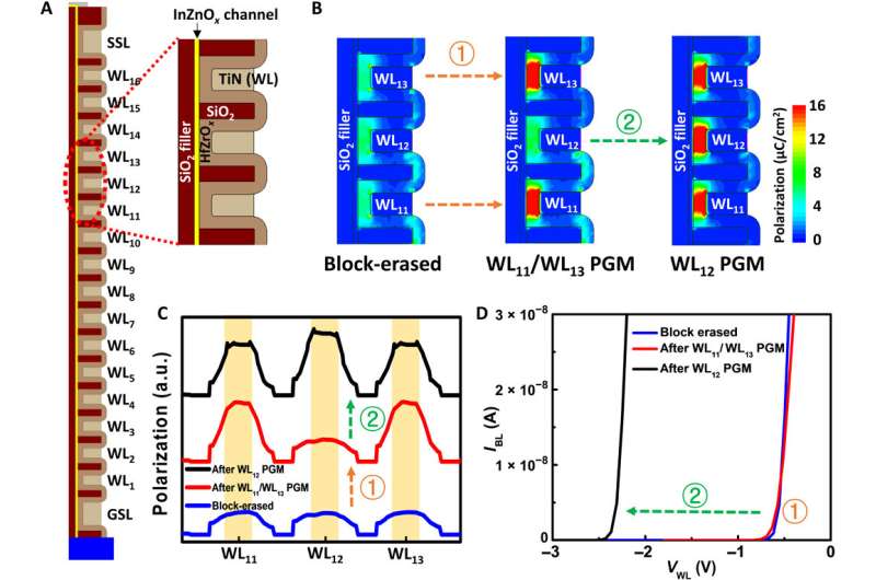
Simulating 3-D FeNAND devices
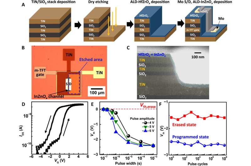
In order to understand the feasibility of ferroelectric thin-film transistors based on zirconium-doped hafnium oxide and indium zinc oxide within future 3-D FeNAND devices, Kim et al. then simulated a single string containing 16-word lines, a string select line and a ground select line. The team thereafter performed block-erase operations to further observe the operation characteristics of the 3-D FeNAND device. In this way, the 3-D FeNAND devices were successfully programmed with highly stacked structures to show that their constituent ferroelectric thin-film transistors maintained low power consumption and fast operation speed to replace 3-D NAND flash memory.
Min-Kyu Kim and colleagues demonstrated a combined ferroelectric oxide semiconductor channel as a unique integration strategy to solve key issues in ferroelectric memory transistors. They tested the potential of the ferroelectric memory as an alternative to conventional flash memory using an integrated FeNAND (ferroelectric NAND) and a vertical ferroelectric thin-film transistor (FeTFT) array. The FeTFTs were functional in the vertical structure and the team confirmed the operation mechanisms via device simulation. They also confirmed the possibility of ultra-high density 3-D memory integration by simulating program and block-erase operational functions in 3-D FeNAND cells. The results suggested the atomic-layer deposition-based FeTFTs to have promising applications in future high-density 3-D memory devices.
Lee C-H. et al. Charge-trapping device structure of SiO2∕SiN∕high-k dielectric Al2O3 for high-density flash memory. Applied Physics Letters, doi.org/10.1063/1.1897431
Cheema S. S. et al. Enhanced ferroelectricity in ultrathin films grown directly on silicon, Nature, doi.org/10.1038/s41586-020-2208-x