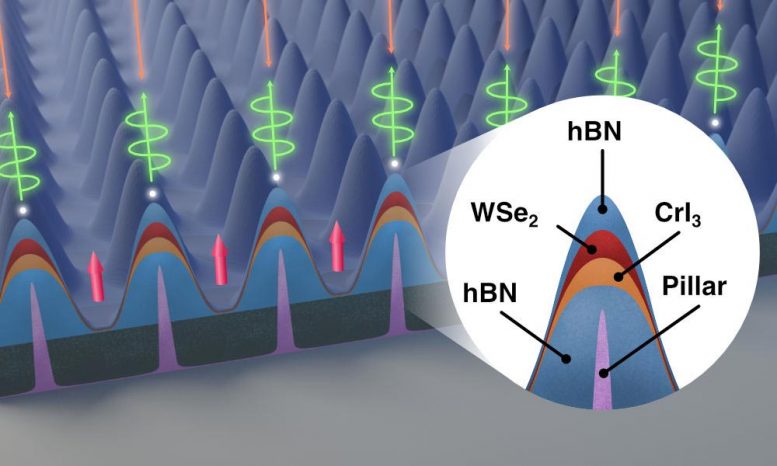
This illustration of a nanoscale node created by the lab of Nick Vamivakas, professor of quantum optics and quantum physics, shows a closeup of one of an array pillars, each a mere 120 nanometers high. Each pillar serves as a location marker for a quantum state that can interact with photons. A novel alignment of tungsten diselenide (WSe2) is draped over the pillars with an underlying, highly reactive layer of chromium triiodide (CrI3). Where the atomically thin, 12-micron area layers touch, the CrI3 imparts an electric charge to the WSe2, creating a “hole” alongside each of the pillars. Credit: University of Rochester illustration / Michael Osadciw
New research demonstrates a way to use quantum properties of light to transmit information, a key step on the path to the next generation of computing and communications systems.
Researchers at the University of Rochester and Cornell University have taken an important step toward developing a communications network that exchanges information across long distances by using photons, mass-less measures of light that are key elements of quantum computing and quantum communications systems.
The research team has designed a nanoscale node made out of magnetic and semiconducting materials that could interact with other nodes, using laser light to emit and accept photons.
The development of such a quantum network—designed to take advantage of the physical properties of light and matter characterized by quantum mechanics—promises faster, more efficient ways to communicate, compute, and detect objects and materials as compared to networks currently used for computing and communications.
Described in the journal Nature Communications, the node consists of an array of pillars a mere 120 nanometers high. The pillars are part of a platform containing atomically thin layers of semiconductor and magnetic materials.
The array is engineered so that each pillar serves as a location marker for a quantum state that can interact with photons and the associated photons can potentially interact with other locations across the device—and with similar arrays at other locations. This potential to connect quantum nodes across a remote network capitalizes on the concept of entanglement, a phenomenon of quantum mechanics that, at its very basic level, describes how the properties of particles are connected at the subatomic level.
“This is the beginnings of having a kind of register, if you like, where different spatial locations can store information and interact with photons,” says Nick Vamivakas, professor of quantum optics and quantum physics at Rochester.
Toward ‘miniaturizing a quantum computer’
The project builds on work the Vamivakas Lab has conducted in recent years using tungsten diselenide (WSe2) in so-called Van der Waals heterostructures. That work uses layers of atomically thin materials on top of each other to create or capture single photons.
The new device uses a novel alignment of WSe2 draped over the pillars with an underlying, highly reactive layer of chromium triiodide (CrI3). Where the atomically thin, 12-micron area layers touch, the CrI3 imparts an electric charge to the WSe2, creating a “hole” alongside each of the pillars.
In quantum physics, a hole is characterized by the absence of an electron. Each positively charged hole also has a binary north/south magnetic property associated with it, so that each is also a nanomagnet.
When the device is bathed in laser light, further reactions occur, turning the nanomagnets into individual optically active spin arrays that emit and interact with photons. Whereas classical information processing deals in bits that have values of either 0 or 1, spin states can encode both 0 and 1 at the same time, expanding the possibilities for information processing.
“Being able to control hole spin orientation using ultrathin and 12-micron large CrI3, replaces the need for using external magnetic fields from gigantic magnetic coils akin to those used in MRI systems,“ says lead author and graduate student Arunabh Mukherjee. “This will go a long way in miniaturizing a quantum computer based on single hole spins. “
Still to come: Entanglement at a distance?
Two major challenges confronted the researchers in creating the device.
One was creating an inert environment in which to work with the highly reactive CrI3. This was where the collaboration with Cornell University came into play. “They have a lot of expertise with the chromium triiodide and since we were working with that for the first time, we coordinated with them on that aspect of it,” Vamivakas says. For example, fabrication of the CrI3 was done in nitrogen-filled glove boxes to avoid oxygen and moisture degradation.
The other challenge was determining just the right configuration of pillars to ensure that the holes and spin valleys associated with each pillar could be properly registered to eventually link to other nodes.
And therein lies the next major challenge: finding a way to send photons long distances through an optical fiber to other nodes, while preserving their properties of entanglement.
“We haven’t yet engineered the device to promote that kind of behavior,” Vamivakas says. “That’s down the road.”
Reference: “Observation of site-controlled localized charged excitons in CrI3/WSe2 heterostructures” by Arunabh Mukherjee, Kamran Shayan, Lizhong Li, Jie Shan, Kin Fai Mak and A. Nick Vamivakas, 30 October 2020, Nature Communications.DOI: 10.1038/s41467-020-19262-2
In addition to Vamivakas and Mukherjee, other coauthors of the paper include lead authors Kamran Shayan of Vamivakas’ lab and Lizhong Li, Jie Shan, and Kin Fai Mak at Cornell University.
The National Science Foundation, the Air Force Office of Scientific Research, and the Department of Energy supported the project with funding.