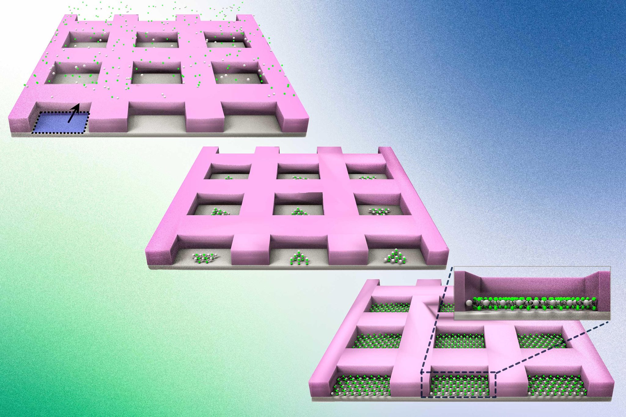
By depositing atoms on a wafer coated in a “mask” (top left), MIT engineers can corral the atoms in the mask’s individual pockets (center middle), and encourage the atoms to grow into perfect, 2D, single-crystalline layers (bottom right). Credit: Jeehwan Kim, Ki Seok Kim, et. al
Their method could enable chip manufacturers to create transistors for the next generation using materials besides silicon.
Adhering to Moore’s Law, the number of transistors on a microchip has doubled annually since the 1960s, but this growth is expected to reach its limit as silicon, the foundation of modern transistors, loses its electrical properties when devices made from it dip below a certain size.
Enter 2D materials — delicate, two-dimensional sheets of perfect crystals that are as thin as a single
But before the electronics industry can transition to 2D materials, scientists have to first find a way to engineer the materials on industry-standard silicon wafers while preserving their perfect crystalline form. And MIT engineers may now have a solution.
The team has developed a method that could enable chip manufacturers to fabricate ever-smaller transistors from 2D materials by growing them on existing wafers of silicon and other materials. The new method is a form of “nonepitaxial, single-crystalline growth,” which the team used for the first time to grow pure, defect-free 2D materials onto industrial silicon wafers.
With their method, the team fabricated a simple functional transistor from a type of 2D materials called transition-metal dichalcogenides, or TMDs, which are known to conduct electricity better than silicon at nanometer scales.
“We expect our technology could enable the development of 2D semiconductor-based, high-performance, next-generation electronic devices,” says Jeehwan Kim, associate professor of mechanical engineering at
Recently, researchers have found other ways to fabricate 2D materials, by growing them on wafers of sapphire — a material with a hexagonal pattern of atoms which encourages 2D materials to assemble in the same, single-crystalline orientation.
“But nobody uses sapphire in the memory or logic industry,” Kim says. “All the infrastructure is based on silicon. For semiconductor processing, you need to use silicon wafers.”
However, wafers of silicon lack sapphire’s hexagonal supporting scaffold. When researchers attempt to grow 2D materials on silicon, the result is a random patchwork of crystals that merge haphazardly, forming numerous grain boundaries that stymie conductivity.
“It’s considered almost impossible to grow single-crystalline 2D materials on silicon,” Kim says. “Now we show you can. And our trick is to prevent the formation of grain boundaries.”
Seed pockets
The team’s new “nonepitaxial, single-crystalline growth” does not require peeling and searching flakes of 2D material. Instead, the researchers use conventional vapor deposition methods to pump atoms across a silicon wafer. The atoms eventually settle on the wafer and nucleate, growing into two-dimensional crystal orientations. If left alone, each “nucleus,” or seed of a crystal, would grow in random orientations across the silicon wafer. But Kim and his colleagues found a way to align each growing crystal to create single-crystalline regions across the entire wafer.
To do so, they first covered a silicon wafer in a “mask” — a coating of silicon dioxide that they patterned into tiny pockets, each designed to trap a crystal seed. Across the masked wafer, they then flowed a gas of atoms that settled into each pocket to form a 2D material — in this case, a TMD. The mask’s pockets corralled the atoms and encouraged them to assemble on the silicon wafer in the same, single-crystalline orientation.
“That is a very shocking result,” Kim says “You have single-crystalline growth everywhere, even if there is no epitaxial relation between the 2D material and silicon wafer.”
With their masking method, the team fabricated a simple TMD transistor and showed that its electrical performance was just as good as a pure flake of the same material.
They also applied the method to engineer a multilayered device. After covering a silicon wafer with a patterned mask, they grew one type of 2D material to fill half of each square, then grew a second type of 2D material over the first layer to fill the rest of the squares. The result was an ultrathin, single-crystalline bilayer structure within each square. Kim says that going forward, multiple 2D materials could be grown and stacked together in this way to make ultrathin, flexible, and multifunctional films.
“Until now, there has been no way of making 2D materials in single-crystalline form on silicon wafers, thus the whole community has almost given up on pursuing 2D materials for next-generation processors,” Kim says. “Now we have completely solved this problem, with a way to make devices smaller than a few nanometers. This will change the paradigm of Moore’s Law.”
Reference: “Non-epitaxial single-crystal 2D material growth by geometric confinement” by Ki Seok Kim, Doyoon Lee, Celesta S. Chang, Seunghwan Seo, Yaoqiao Hu, Soonyoung Cha, Hyunseok Kim, Jiho Shin, Ju-Hee Lee, Sangho Lee, Justin S. Kim, Ki Hyun Kim, Jun Min Suh, Yuan Meng, Bo-In Park, Jung-Hoon Lee, Hyung-Sang Park, Hyun S. Kum, Moon-Ho Jo, Geun Young Yeom, Kyeongjae Cho, Jin-Hong Park, Sang-Hoon Bae and Jeehwan Kim, 18 January 2023, Nature.DOI: 10.1038/s41586-022-05524-0
The study was funded by
Source: SciTechDaily
I was very pleased to uncover this great site. I need to to thank you for ones time for this fantastic read!! I definitely appreciated every bit of it and I have you bookmarked to look at new information on your blog.
Id like to thank you for the efforts you have put in penning this site. Im hoping to see the same high-grade blog posts by you in the future as well. In fact, your creative writing abilities has inspired me to get my own site now 😉