A Q&A with two scientists aiming to overcome limits in computing power and energy efficiency by designing new microchips.
Our laptops and smartphones are compact yet powerful because of silicon microelectronics, also known as microchips or chips, the tiny brains behind the digital brawn of almost every modern device.
But such modern convenience comes at a cost. By 2030, about 25% of the world’s energy – most of which is produced by burning carbon-rich fossil fuels – could be consumed by electronic devices if nothing is done to make them more energy efficient.
Silicon chips originate from a design known as CMOS, shorthand for complementary metal-oxide-semiconductor. As Moore’s Law first predicted in 1975, CMOS silicon chips are approaching limits in miniaturization and performance. For decades, scientists have been on the hunt for new electronic materials that go beyond the limits of Moore’s Law as well as the constraints of silicon CMOS chips.
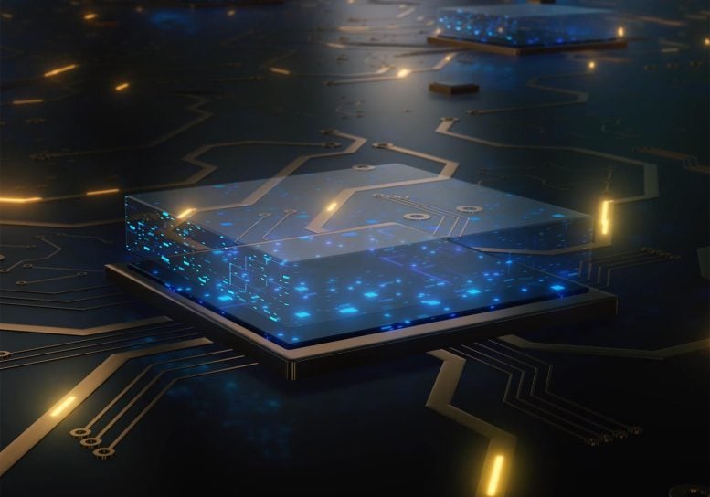
Now, scientists Maurice Garcia-Sciveres and Ramamoorthy Ramesh at DOE’s Lawrence Berkeley National Laboratory (Berkeley Lab) are designing new microchips that could perform better – and require less energy – than silicon. Over the next three years, they will lead two of the 10 projects recently awarded nearly $54 million by the Department of Energy to increase energy efficiency in microelectronics design and production.
They discuss their projects in this Q&A.

Berkeley Lab scientists Maurice Garcia-Sciveres (left) and Ramamoorthy Ramesh are designing new microchips that could perform better – and require less energy – than silicon. Credit: Courtesy of Garcia-Sciveres and Ramesh
Q: Over the next 3 years, what do you hope to achieve? What is the significance of your work?
Garcia-Sciveres: Our project – the “Co-Design and Integration of Nano-Sensors on CMOS” – aims to improve performance by integrating tiny light sensors made with nanomaterials into a conventional CMOS (complementary metal-oxide-semiconductor) integrated circuit. (A nanomaterial is matter designed at an ultrasmall scale of a billionth of a meter.)
CMOS chips are made of silicon, but if you look at how much power silicon uses, it’s starting to be significant – and in a decade, silicon chips will be consuming a large fraction of our energy. For example, the computing needed to run a self-driving car consumes significant energy compared to the energy needed to run the car. We need to compute with less energy, or increase performance without more power, but you can’t do that with silicon chips because silicon has to run on a certain voltage – and those physical limitations are costing us.
In our project, nanomaterials such as carbon nanotubes – devices so small that they are invisible to the naked eye – would serve as light sensors. The nanosensors add new functionality to a CMOS chip, increasing performance.
Sensing is a good initial application, but when integrated into a chip, the carbon nanotubes could also serve as transistors or switches that process data. Integrating many carbon nanotubes into a silicon chip could lead to new kinds of electronic devices that are smaller and faster as well as more energy efficient than current technologies.
Ramesh: In our project, “Co-Design of Ultra-Low-Voltage Beyond CMOS Microelectronics,” we plan to explore new physical phenomena that will lead to significantly higher energy efficiency in computing. This is important because we believe that the next Moore’s Law is likely to be focused on the energy scale and not the length scale, since we are already at the limits of length scaling.
In around 2015, energy consumption from microelectronics was only about 4-5% of the world’s total primary energy. Primary energy typically means the chemical energy produced by a coal- or natural gas-based power plant. This typically has an efficiency of conversion to electricity of 35-40%.
Our increasing reliance on artificial intelligence, machine learning, and IoT – or the Internet of Things where everything is electronically connected, such as our traffic systems, emergency response systems, and renewable energy and electrical grid systems – will lead to an exponential increase of electronics from the systems perspective.
This means that by 2030, energy consumption from microelectronics is projected to be at least 25% of primary energy. Therefore, making electronics more energy efficient is a big deal.
For our project, we are asking, “What fundamental materials innovations could significantly scale back the energy consumption of microelectronics?” We’re looking at a totally different framework that explores new physics using a co-design approach, in which world-leading experts in materials physics, device and circuit design, fabrication and testing, and chip-level architecture are working in collaboration to carry out a holistic study of pathways to next-generation computing.
Q: What new applications will your work enable, and how will you demonstrate these new capabilities?
Garcia-Sciveres: Our work will demonstrate a single-photon imager that can measure the spectrum – the wavelength or energy – of every single photon or light particle it detects. This allows for hyperspectral imaging – that is, images where each pixel can be decomposed into many colors, providing much more information. Hyperspectral imaging benefits a broad range of science, from cosmology to biological imaging.
The Dark Energy Spectroscopic Experiment (